完善资料让更多小伙伴认识你,还能领取20积分哦, 立即完善>


 1937人已学习
 4347人已学习
 5893人已学习
 773人已学习

开源芯片系列讲座第22期:异步电路机制为RISC-V处理器赋能

PerfxCloud 大模型人工智能创新威廉希尔官方网站 大会

共建RISC-V生态——RISC-V单板计算机的创新开发与实践

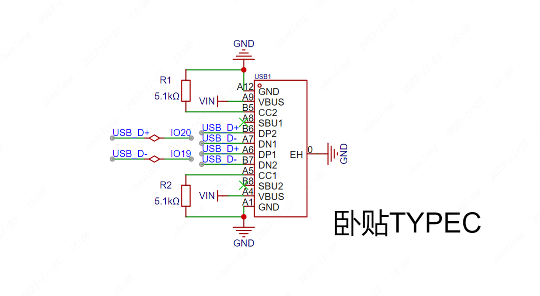
本规范规定公司所设计PCB板期间封装的命名与设计规范度,保证公司设计的PCB板器件使用的统一性,便于对所设计的PCB可靠性进行监控,也极便于对PCB审核与归档。下载本书后,推荐配合使用华秋DFM,用于对元器件进行可组装性分析,让PCB设计0错误。 华秋DFM下载地址(电脑版):https://dfm.elecfans.com/uploads/software/promoter/hqdfm_fany.zip

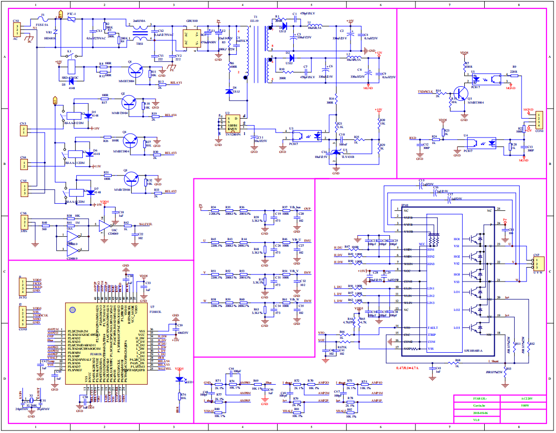
本期电子发烧友《开关电源噪声—EMC》为您讲解关于开关电源噪声—EMC的一些常用技巧,本电子书围绕“开关噪声-EMC”这一主题,对开关电源相关的 EMC 及其对策等进行解说。本部分为电子书的下部分,主要介绍如何降低噪声,为大家介绍如何使用电容器降低噪声,使用电感降低噪声。

本期电子发烧友《开关电源噪声—EMC》为您讲解关于开关电源噪声—EMC的一些常用技巧,本电子书围绕“开关噪声-EMC”这一主题,对开关电源相关的 EMC 及其对策等进行解说。先介绍了 EMC 相关的基础知识,然后再探讨噪声对策相关的内容。
jf_17362901 4秒前 下载了
jf_17362901 1分钟前 下载了
jf_45666886 2分钟前 下载了
jf_17362901 2分钟前 下载了
jf_85290803 3分钟前 下载了
jf_17362901 4分钟前 下载了
已有 544192 份资料
| 今日更新:129个 | 内容总数:544192 |
| 今日下载:651个 | 30日更新:18239个 |
| 资源总大小:1411.01G | 资源总下载:6531233次 |
2024-03-27线上直播
2024-06-26线上直播


 价iPhone果然抢手!安卓转投iPhone比例创五年来新高