基于MC33905设计的MCU功率管理方案
Freescale 公司的MC33905是第二代系统基本芯片(SBC),包括有多中特性和增强的模块设计,能作为MCU和其它集成电路如传感器,CAN收发器的先进的功率管理单元. MC33905内置了高速CAN接口(ISO11898-2 和-5),以及本地和总线故障诊断,保护以及故障安全操作模式等.本文介绍了MC33905主要特性,方框图,以及简化应用框图和典型应用电路, MC33905评估板EVB主要特性, 电路图和材料清单(BOM).
The 33904/5 is the second generation family of System Basis Chips which combine several features and enhance present module designs. The device works as an advanced power management unit for the MCU and additional integrated circuits such as sensors, CAN transceivers. It has a built-in enhanced high speed CAN interface (ISO11898-2 and -5), with local and bus failure diagnostics, protection, and fail safe operation mode. The SBC may include one or two LIN 2.1 interfaces with LIN output pin switches. It includes up to 4 wake-up input pins than can also be configured as output drivers for flexibility.
This device implements multiple Low Power modes, with very low-current consumption. In addition, the device is part of a family concept where pin compatibility, among the various devices with and without LIN interfaces, add versatility to module design.
The 33904/5 also implements an innovative and advanced fail-safe state machine and concept solution.
MC33904/5主要特性:
•Protected 5.0V or 3.3V regulators for MCU (part number selectable) and additional ICs (SPI configurable) with optional external PNP usage to increase current capability for MCU.
•Fully-protected embedded 5.0 V regulator for the CAN driver
•Extremely low quiescent current in low power modes
•Multiple under-voltage detections to address various MCU specifications and system operation modes (i.e. cranking)
•Multiple wake-up sources in low power modes: CAN or LIN bus, I/O transition, automatic timer, SPI message, and VDD over-current detection.
•Voltage, current and temperature protection with enhanced diagnostics that can be monitored by system via MUX output
•ISO11898-5 high speed CAN interface compatibility for baud rates of 40 kb/s to 1.0 Mb/s. LIN 2.1 and J2602 LIN interface compatibility
•Pb-free packaging designated by suffix code EK 
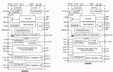
图1.MC33905D内部方框图 
图2.MC33905S内部方框图 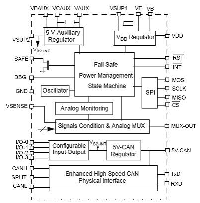
图3.MC33904A内部方框图 
图4.MC33905D简化应用方框图 
图5.MC33905S简化应用方框图 
图6.MC33905A简化应用方框图 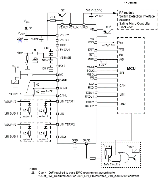
图7.MC33905D典型应用电路图 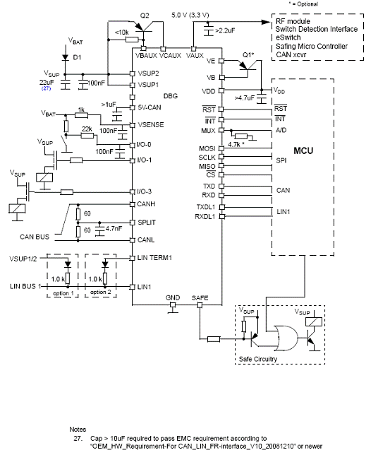
图8.MC33905S典型应用电路图 
图9.MC33905A典型应用电路图
MC33905评估板EVB
This EVB includes two I/O test points that can be configured to be pulled up to VSup or pulled down to GND through a resistor and indicator LED. These are easily configured via jumper settings. The SBC can also be exercised in debug mode (watchdog re-fresh/monitoring not needed) by simply populating a jumper. Separating the input supply voltage to VSup1 and VSup2 is also made simple with a jumper configuration. Specified resistor pull-downs can be implemented on DBG and MUX pins via simple jumper configurations. The status of I/O0, I/O1, VAUX, 5V_CAN, SAFE and VDD can be visually monitored via on-board LEDs. The CAN and LIN Bus signals are provided through terminal block connectors.
An isolated terminal block connector is implemented to provide power to the evaluation board with an external DC power supply.
The evaluation board is operated through the graphical user interface paired up with the SPI dongle board (KITUSBSPIDGLEVME) through the 2x8 pin ribbon cable. Additionally, for added flexibility, the user can implement a custom board with a microcontroller to talk to the SBC via the 16 pin header.
MC33905评估板EVB主要特性:
•Nominal operating supply voltage range of 5.5V to 27V
•Individually routed power supply inputs for VSup1 and VSup2
•5.0 V regulator for MCU with external PNP ballast transistor to increase current capability.
•Multiple CAN Bus termination options supported via socket
•Two high/low side I/Os (SPI configurable) accessible through test points.
•Status of I/O0 and I/O1 indicated by LED (dependent on jumper configuration)
•Debug Mode/watchdog configuration via jumper settings
•MUX output voltage accessible through test point and external resistor selectable through jumper
•3.3 V or 5.0 V output voltage test point VAUX (SPI configurable)
•I_WAKE_I test point to enable a FET and load VDD with current to wake up the SBC.
•LIN1_T and LIN2_T test points to monitor I/O voltages (SPI configurable)
•I/O0, I/O1, VAUX, 5V_CAN, SAFE and VDD status indicated by LED
•100mil 2x8-pin standard header connector for SPI communication
•100mil 16-pin standard header connector for custom MCU board connection
图10.MC33905评估板KIT33905D5EKEVBE外形图
图11.评估板KIT33905D5EKEVBE建立配置方框图
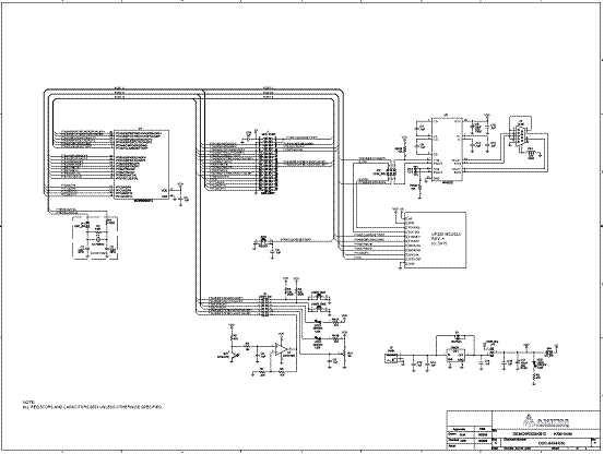
图12.评估板KIT33905D5EKEVBE电路图
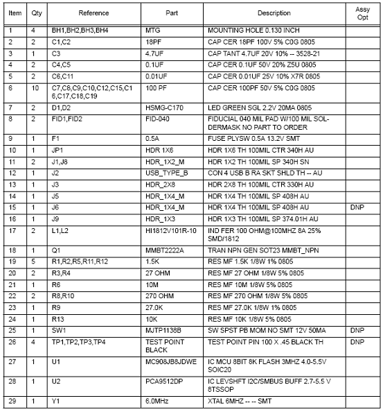
评估板KIT33905D5EKEVBE材料清单(BOM):
 电子发烧友App







评论