 电子发烧友App


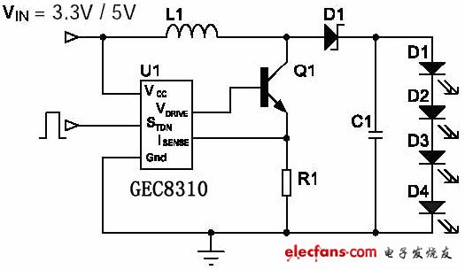
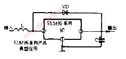
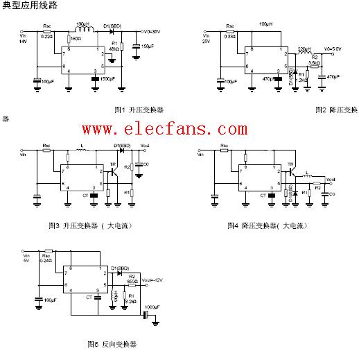
GEC8310典型应用电路


相关推荐

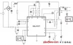
基于GEC8310的高电池寿命LED电路
为了提高效率,使电池寿命达到最大,LED 的驱动电流为脉冲电流,并且去掉了整流电路。所谓脉冲电流,是由于没有输出电容,LED 只是在开关管断开时才有驱动电流,开关管导通时则
2012-04-13 09:26:45 1924
1924
1924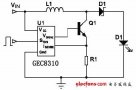
基于GEC8310的高亮度LED电路
该电路通过对于DC-DC 输出进行整流和缓冲为单个LED 提供持续的驱动电流,从而保证最大的LED 亮度。基于 GEC8310 的高亮度LED电路:
2012-04-13 09:24:292074
2074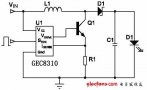
基于GEC8310的LCD背光电路
这是一种典型的LCD 背光应用,输入电压通常为主系统电源,典型值3.3V 或5V.LED 为串联形式,以使发光均匀。LED 的驱动电流既可以是脉冲也可以是直流。LED 的驱动电流的大小可由感应电
2012-04-13 09:22:072066
2066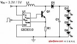
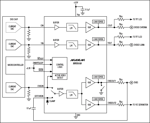
液晶显示器背光源LED驱动器GEC8310方案
GEC8310 是一个作为LCD背光的单个或多个LED的驱动器,其工作输入电压范围在0.85V 至8V之间。
2012-04-13 09:15:452253
2253


AD8310的典型应用连接图
AD8310的基本参考电路图
AD8310的高增益和宽带宽使得它对输入端极宽频率范围内的所有信号都非常敏感。因此,不用滤波器将很难区别出所需的信号,并
2009-12-08 10:16:413310
3310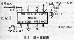


集成基准电压源典型应用电路
集成基准电压源典型应用电路
1. LM399 典型应用电路图18-18 是LM399 集成基准电压源的典型应用电路。在实际使用中,可以把基准电压部分看作是一个稳压管,因此在
2009-09-19 15:39:121697
1697


OPA678的典型应用电路图
OPA678的典型应用电路图
以下是OPA678的4个典型应用电路。图中CDC是电源去耦电容,为1μF的钽电容;为防止其高频时的电感效应,再并联一个
2009-03-14 16:54:131127
1127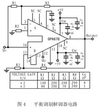


 工商网监
工商网监
评论