Abstract: This application note describes how to use the DS1670 Portable System Controller, a 3-wire serial interface real-time clock (RTC). The DS1670 supplies features that are targeted at portable (hand held) systems.
Key functions frequently required in portable products include a real time clock; nonvolatile RAM control to ensure that data is not lost in the event of a power-down or battery-fail; microprocessor monitoring to ensure that the microprocessor does not "run out of control"; and analog-to-digital converters for interfacing with external environmental sensors, battery monitoring, etc. The DS1670 Portable System Controller replaces as many as four separate integrated circuits by incorporating all of these functions in a single device. The DS1670 provides a very accurate real time clock, nonvolatile SRAM controller, microprocessor monitor, and 3-channel 8-bit analog-to-digital converter. Communication with the device is established through a simple 3-wire interface.
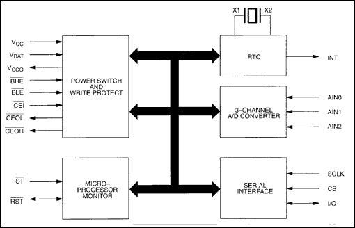
Figure 1. DS1670 block diagram.
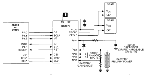
Figure 2. Typical application.
An A/D conversion is the process of assigning a digital code to an analog input voltage. This code represents the input value as a fraction of the full scale voltage (FSV) range. Thus the FSV range is then divided by the A/D converter into 256 codes (8 bits). The FSV range is bounded by an upper limit equal to the reference voltage and the lower limit, which is ground. The DS1670 has a FSV of 2.55V (typically) which provides a resolution of 10 mV. An input voltage equal to the reference voltage converts to FFh while an input voltage equal to ground converts to 00h. The relative linearity of the A/D converter is ±0.5 LSB.
The analog input (AIN0, AIN1, or AIN2) for an analog-to-digital conversion is selected by the condition of the Analog Input Select (AIS) bits in the Control Register. Conversions occur every 10 ms and the result is placed in the ADC Register.
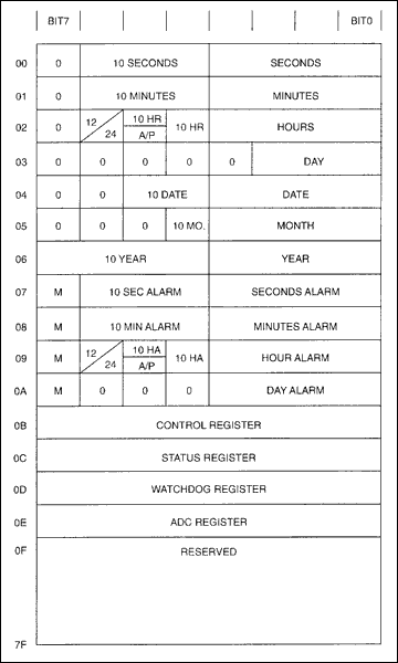
Figure 3. DS1670 address map.
Power to the SRAMs is provided from the VCCO pin of the DS1670. When VCC is within nominal limits (greater than 2.7 volts typical), VCCO is internally connected to VCC. However, when VCC goes below nominal limits, VCCO is internally connected to VBAT, thus ensuring that the SRAM data is maintained in the event of a primary power supply failure. VBAT is typically connected to a lithium battery, rechargeable battery, or super capacitor. Figure 3 illustrates VBAT connected to a super capacitor. The super capacitor is charged whenever the power source connected to VCC is a diode drop above VBAT plus the voltage drop across resistor R1. R1 is used to decrease the charge current to the super capacitor. Note that in this application, the primary power source connected to VCC is a battery. This could be a rechargeable battery pack or perhaps a series of AA cells. Regardless of the type of battery used, the DS1670 allows the battery to be changed without the loss of important data. Depending on the size and type of super capacitor or battery connected to VBAT, the data will be saved from several hours to several years without replacing the main system battery. It should be noted also that when using a super capacitor, the limiting factor is often the internal leakage of the capacitor itself. In other words, the battery back-up current consumed by the DS1670 and SRAMs is negligible compared to the internal leakage of the capacitor.
Features
There is an increasing trend in the industry today towards portable battery-operated products. These products typically require extremely small form factors and low power. The DS1670 Portable System Controller is designed to help the portable system designer in meeting these two requirements by integrating key functions typically needed in these systems while consuming very little power.Key functions frequently required in portable products include a real time clock; nonvolatile RAM control to ensure that data is not lost in the event of a power-down or battery-fail; microprocessor monitoring to ensure that the microprocessor does not "run out of control"; and analog-to-digital converters for interfacing with external environmental sensors, battery monitoring, etc. The DS1670 Portable System Controller replaces as many as four separate integrated circuits by incorporating all of these functions in a single device. The DS1670 provides a very accurate real time clock, nonvolatile SRAM controller, microprocessor monitor, and 3-channel 8-bit analog-to-digital converter. Communication with the device is established through a simple 3-wire interface.
Using the DS1670
The DS1670 can be directly interfaced with any microprocessor or microcontroller through a 3-wire serial interface. The serial interface gives the microprocessor access to the DS1670 registers, which consist of the Real Time Clock Registers, Control Register, Status Register, Watchdog Register, and ADC (Analog-to-Digital Converter) Register. Figures 1 and 2 illustrate a block diagram and address map of the DS1670, respectively. The following paragraphs briefly describe the operation of the various components of the DS1670 as well as the functions of the various control and status registers. For more detailed information, please consult the DS1670 data sheet.
Figure 1. DS1670 block diagram.

Figure 2. Typical application.
Real Time Clock
The Real Time Clock (RTC) provides seconds, minutes, hours, day, date, month, and year information with leap year compensation. The RTC has a back-up power supply input (VBAT) that enables it to continue to keep time even when the primary supply connected to VCC is removed. The RTC also provides an alarm interrupt which is functional both when the DS1670 is powered by the system power supply or when in battery back-up operation. Functionality while in battery back-up operation allows the alarm to "wake up" a system that is powered down.Nonvolatile SRAM Control
The nonvolatile SRAM controller of the DS1670 provides two important functions. First, it ensures a constant uninterrupted power supply to the system SRAMs. This is provided by the VCC Output pin (VCCO). VCCO is internally connected to VCC when VCC is within nominal limits. However, when VCC is below nominal limits, VCCO is connected to the power source connected to VBAT (typically a lithium battery, rechargeable battery, or super capacitor). The second important feature of the nonvolatile controller is that it gates the chip enable signals to the SRAMs. This ensures that the microprocessor can access the SRAMs only when the primary power supply is within nominal limits, thus eliminating the corruption of data during power transients. It should also be noted that the DS1670 provides nonvolatile control for two separate SRAMs. The two inputs from the microprocessor are Byte High Enable (active-low BHE) and Byte Low Enable (active-low BLE). These inputs correspond to the two output Chip Enable Output High (active-low CEOH) and Chip Enable Output Low (active-low CEOL).Microprocessor Monitor
The microprocessor monitor circuitry of the DS1670 provides three basic functions:- A precision temperature-compensated reference and comparator circuit monitors the status of VCC. When an out-of-tolerance condition occurs, an internal power fail signal is generated which forces the reset to the active state. When VCC returns to an in-tolerance condition, the reset signals are kept in the active state for 250 ms to allow the power supply and processor to stabilize.
- Pushbutton reset control: The DS1670 debounces a pushbutton input and guarantees an active reset pulse width of 250 ms.
- Watchdog timer: The DS1670 has an internal timer that forces the reset signals to the active state if the strobe input is not driven low prior to watchdog time-out.
Analog-to-Digital Converter
The DS1670 also provides a 3-channel 8-bit successive approximation analog-to-digital converter. The converter has an internal 2.55 volt (typical) reference voltage generated by an on-board band-gap circuit. The A/D converter is monotonic (no missing codes) and has an internal analog filter to reduce high frequency noise.An A/D conversion is the process of assigning a digital code to an analog input voltage. This code represents the input value as a fraction of the full scale voltage (FSV) range. Thus the FSV range is then divided by the A/D converter into 256 codes (8 bits). The FSV range is bounded by an upper limit equal to the reference voltage and the lower limit, which is ground. The DS1670 has a FSV of 2.55V (typically) which provides a resolution of 10 mV. An input voltage equal to the reference voltage converts to FFh while an input voltage equal to ground converts to 00h. The relative linearity of the A/D converter is ±0.5 LSB.
The analog input (AIN0, AIN1, or AIN2) for an analog-to-digital conversion is selected by the condition of the Analog Input Select (AIS) bits in the Control Register. Conversions occur every 10 ms and the result is placed in the ADC Register.
Typical Application
Figure 3 illustrates a typical application using the DS1670. In this application, the DS1670 is shown interfacing with a 386EX or 80186 microprocessor (microprocessors designed with embedded applications in mind). Communication between the microprocessor and the DS1670 is accomplished easily through three port pins (P1.0-P1.2) which are connected to the 3-wire serial interface pins of the DS1670 Serial Clock (SCLK), Chip Select (active-low CS), and serial input/output (I/O). This serial interface provides access to the real time clock, ADC, control, and status registers of the DS1670.
Figure 3. DS1670 address map.
Nonvolatile SRAM Control
The DS1670 also provides nonvolatile control of external SRAMs in this circuit example. The Chip Select (active-low CS), Byte High Enable (active-low BHE), and Byte Low Enable (active-low BLE) outputs of the microprocessor are gated through the DS1670 to its Chip Enable Output Low (active-low CEOL) and chip Enable Output High (active-low CEOH) output pins. The active-low CEOL and CEOH pins can be driven to the active state only when VCC is within nominal limits (>2.88V) thus preventing the system from receiving or writing corrupted data. Note that the structure of the SRAM access controller allows the microprocessor to access data in worldwide format (16 bits wide by enabling active-low CEOL and active-low CEOH simultaneously) or byte-wide format (8-bit wide by enabling either active-low CEOL or active-low CEOH).Power to the SRAMs is provided from the VCCO pin of the DS1670. When VCC is within nominal limits (greater than 2.7 volts typical), VCCO is internally connected to VCC. However, when VCC goes below nominal limits, VCCO is internally connected to VBAT, thus ensuring that the SRAM data is maintained in the event of a primary power supply failure. VBAT is typically connected to a lithium battery, rechargeable battery, or super capacitor. Figure 3 illustrates VBAT connected to a super capacitor. The super capacitor is charged whenever the power source connected to VCC is a diode drop above VBAT plus the voltage drop across resistor R1. R1 is used to decrease the charge current to the super capacitor. Note that in this application, the primary power source connected to VCC is a battery. This could be a rechargeable battery pack or perhaps a series of AA cells. Regardless of the type of battery used, the DS1670 allows the battery to be changed without the loss of important data. Depending on the size and type of super capacitor or battery connected to VBAT, the data will be saved from several hours to several years without replacing the main system battery. It should be noted also that when using a super capacitor, the limiting factor is often the internal leakage of the capacitor itself. In other words, the battery back-up current consumed by the DS1670 and SRAMs is negligible compared to the internal leakage of the capacitor.
 电子发烧友App






评论