PMU Mode Operation for the MAX9979 Pin-Electronics IC
Abstract: This application note describes the operation of four of the most popular operating modes (FVMI, FVMV, FIMI, and FIMV) for the MAX9979's parametric measurement unit (PMU) by referencing the equivalent schematic for each mode. Refer to the MAX9979 data sheet for a full description of all features and modes of operation.
Introduction
The MAX9979 is a highly integrated, dual-channel, pin-electronics (PE) IC for the automatic tester equipment (ATE) market. This design includes a dual, four-level, high-speed, driver/comparator/load (DCL) design with integrated clamps that can be placed into drive, high-impedance, and low-leakage modes. The operating speed exceeds 1 gigabit per second (1Gbps). The design includes the full integration of all levels through individual 16-bit internal digital-to-analog converters (DACs). Each channel also includes a fully integrated, parametric measurement unit (PMU), which has very accurate measurement capabilities and is a valuable addition to the design.
PMU Modes of Operation
The MAX9979's PMU has many modes of operation. However, only four (FVMI, FVMV, FIMI, and FIMV) are discussed in this application note.
Table 1 shows how to set the PMU for its four main modes. FMODE, MMODE, and active-low HIZFORCE are controlled by the internal serial interface. Active-low LLEAKP is an external pin.
Table 1. PMU Mode Selection
| PMU Mode | Driver | Comparator | Load | FMODE | MMODE | Active-Low LLEAKP | Active-Low HIZFORCE |
| FVMI | Low-leak | Low-leak | Low-leak | 0 | 0 | 1 | 1 |
| FVMV | 0 | 1 | 1 | 1 | |||
| FIMI | 1 | 0 | 1 | 1 | |||
| FIMV | 1 | 1 | 1 | 1 |
Force Voltage Measure Current (FVMI)
In FVMI mode, an internally generated voltage (VIN) is forced directly on the device-under-test (DUT) output pin. VIN can be programmed from -2.5V to +7.5V with a resolution of 16 bits through the serial interface, though its valid range is -1.5V to +6.5V. Programming VIN outside this valid range does not harm the MAX9979.
The voltage forced at the DUT node creates a current into or out of the DUT node. This current is monitored and measured at the MEAS pin, and it can be calculated as follows:
where ILOAD is the current into or out of the DUT node, VMEAS is the forced voltage, and VIIOS is the offset programmed voltage. The serial interface bits RS0, RS1, and RS2 (shown in Table 2) internally select the range resistors (RSENSE).
Table 2. PMU Current-Range Control
| Digital Input | Serial Interface Bits | Range (RSENSE) | |||
| Active-Low LLEAKP | Active-Low HIZFORCE | RS2 | RS1 | RS0 | |
| X | X | 0 | 0 | 0 | E (500kΩ ±2µA) |
| X | X | 0 | 0 | 1 | D (50kΩ ±20µA) |
| X | X | 0 | 1 | 0 | C (5kΩ ±200µA) |
| X | X | 0 | 1 | 1 | B (500Ω ±2mA) |
| X | 0 | 1 | X | X | B* |
| 0 | 1 | 1 | X | X | B* |
| 1 | 1 | 1 | X | X | A (20Ω ±50mA) |
Note that VIIOS can be programmed from 0 to +5V, but the valid range has been set from +2V to +4V. Programming outside this valid range also does not harm the MAX9979.
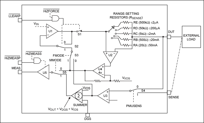
In Figure 1 and Table 1, VIN is the forced input voltage, and it is set by an internal DAC. The DUT node is forced to the programmed VIN through the closed feedback loop of U1, S1, S4, U3, S3, and S2. Controlled by the external SENSE pin, S4 allows the option to sense the load point directly. If S4 is closed, VIN is forced at the load. By using this option, offset voltages errors due to board routings are removed.

Figure 1. Force voltage measure current (FVMI).
U2, U4, S5, and U6 are not in the feedback loop, but provide a path for the MEAS pin to monitor the load current. The voltage that appears at the MEAS pin is calculated using Equation 1.
Table 3 lists some examples of setups for FVMI mode.
Table 3. Examples of FVMI Mode Setups
| VIN (V) |
VIIOS (V) |
Range |
DUT Voltage (V) |
VMEAS (V) |
Load (kΩ) |
Load Current (µA) |
| +1 | +2.5 | D (±20µA) | +1 | +6.5 | 50 | +20 |
| 0 | +2.5 | D (±20µA) | +1 | +2.5 | 50 | 0 |
| -1 | +4 | D (±20µA) | -1 | 0 | 50 | -20 |
Force Voltage Measure Voltage (FVMV)
FVMV mode operates similarly to FVMI mode. VIN is forced at the DUT node (or the external load, if S4 is closed). The difference is in the measure path. Switch S5 is closed, and the MEAS pin now monitors the forced voltage. The MEAS pin can be offset by an internal voltage level called VIOS. VIOS can be programmed from -0.75V to +3.75V, but its valid range is specified to be 0 to +1.5V. By programming VIOS to +1.5V, the MEAS pin can be offset by +1.5V and allow the use of an external unipolar ADC. In this way, the DUT range of -1.5V to +6.5V can be mapped to a 0 to +8V range on the MEAS pin.
Figure 2 differs from Figure 1 in that its mode switch is set to MMODE = 1. The MEAS pin is monitoring the voltage at the DUT node, as well as the ground-sense voltage (at the DGS pin) and VIOS. The feedback loop is the same as the FVMI loop—specifically U1, S1, S4, U3, S3, and S2.
Figure 2. Force voltage measure voltage (FVMV).
The measurement path now consists of S4, U3, S5, and U5 to monitor voltage. Note that S5 is in the "1" position, or MMODE = 1.The MEAS pin can be offset by an internally set VIOS in order to accommodate a unipolar analog-to-digital converter (ADC).
The MEAS pin can also be offset by any difference in ground potential through the DGS pin. The DGS pin can sense the load ground, which helps to eliminate any errors due to ground offsets. Similarly, the SENSE pin can also be set to sense the load directly.
Table 4 lists some examples of setups for FVMV mode.
Table 4. FVMV Mode Setup Examples
| VIN (V) |
VIOS (V) |
Voltage at DGS (V) |
DUT Voltage (V) |
VMEAS (V) |
| -1.5 | 0 | 0 | -1.5 | -1.5 |
| -1.5 | +2 | -0.5 | -1.5 | 0 |
| -1.5 | +1.5 | 0 | -1.5 | 0 |
| +6.5 | +1.5 | 0 | +6.5 | +8 |
The last two setups in Table 4 are designed with a VIOS of 1.5V. The MEAS voltage range is unipolar (0 to 8V) for a -1.5V to +6.5V programmed input. This table shows how to use VIOS so that any ADC can be connected to the MEAS pin.
Figures 1 and 2 show that a customer can have many MEAS pins from a number of MAX9979s all connected together and sharing just one ADC. Each MEAS output can be placed in a high-Z state by the internal serial interface bit, internal active-low HiZMEASS, or external active-low HiZMEASP pin. The customer must assert the high-Z function for the individual device intended to make the measurement.
Force Current Measure Current (FIMI)
In FIMI mode, VIN is forced directly across the internally selected RSENSE resistor. VIN forces a current through this resistor—this current is calculated as shown in Equation 2. A programmed voltage of +1V represents the full-scale range (FSR) for that particular range. (See Table 2 for range selection.) For example, if we select Range D, an RSENSE of 50kΩ, VIN equal to 1V, and a VIIOS of 0V, we then find the forced current (IFORCE) to be 20µA using the following equation:
Therefore, 20µA is specified to be the FSR for Range D.
Note that, when VIIOS equals VIN, the forced current is 0µA. VIIOS can be programmed from 0 to +5V, but its valid range is +2V to +4V. As in FVMI, programming outside of this range does not harm the MAX9979. VIIOS can be considered the zero forced current voltage. It typically should be set to +2.5V, the same as the internally generated reference. The main function of VIIOS is to set the MEAS pin voltage to be compatible with many different ADCs, such as a unipolar ADC.
As shown in Figure 3, the feedback loop for FIMI mode consists of U1, S1, U2, U4, S3, and S2.
Figure 3. Force current measure current (FIMI).
Care must be taken in selecting the correct load to ensure that the output compliance of +6.5V, or -1.5V, is not exceeded. Table 5 shows some FIMI setup options.
Table 5. Setup Examples for FIMI Mode
| VIN (V) |
VIIOS (V) |
Range | DUT Voltage (V) |
VMEAS (V) |
Load (kΩ) |
Load Current (µA) |
| +2.5 | +2.5 | D (±20µA) | 0 | +2.5 | 50 | 0 |
| +6.5 | +2.5 | D (±20µA) | +1.5 | +6.5 | 50 | +20 |
| -1.5 | +2.5 | D (±20µA) | -1 | -1.5 | 50 | -20 |
| -1.5 | +2 | D (±20µA) | -0.875 | -1.5 | 50 | -17.5 |
Force Current Measure Voltage (FIMV)
FIMV mode has the same feedback loop as described in the FIMI mode description. Thus the equation for forcing the current remains the same. For FIMV mode, MMODE is set to 1. As seen in Figure 4, the MEAS pin now monitors the DUT voltage, since S5 is now set to 1.
Table 5 can be used for FIMV setup examples, with the difference being that the VMEAS column would be exactly the same as the DUT voltage column. In other words, the MEAS pin is monitoring the DUT output.
Figure 4. Force current measure voltage (FIMV).
 电子发烧友App







评论